- 您现在的位置:买卖IC网 > Sheet目录328 > IDT7008L25G (IDT, Integrated Device Technology Inc)IC SRAM 512KBIT 25NS 84PGA
IDT7008S/L
High-Speed 64K x 8 Dual-Port Static RAM
Military, Industrial and Commercial Temperature Ranges
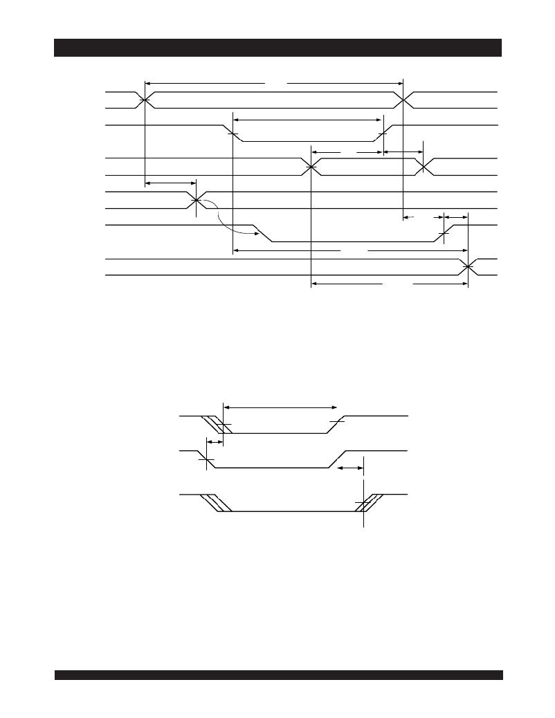
Timing Waveform of Write with Port-to-Port Read and BUSY (2,5) (M/ S = V IH ) (4)
t WC
ADDR "A"
MATCH
t WP
R/ W "A"
DATA IN "A"
t DW
VALID
t DH
ADDR "B"
t APS
(1)
MATCH
BUSY "B"
t WDD
t BDA
t BDD
DATA OUT "B"
NOTES:
t DDD
(3)
VALID
3198 drw 13
1. To ensure that the earlier of the two ports wins. t APS is ignored for M/ S = V IL (SLAVE).
2. CE L = CE R = V IL, refer to Chip Enable Truth Table.
3. OE = V IL for the reading port.
4. If M/ S = V IL (SLAVE), then BUSY is an input ( BUSY "A" = V IH and BUSY "B" = "don't care", for this example).
5. All timing is the same for left and right ports. Port "A" may be either the left or right port. Port "B" is the port opposite from port "A".
Timing Waveform of Write with BUSY (M/ S = V IL )
t WP
R/ W "A"
t WB (3)
BUSY "B"
t WH (1)
R/ W "B"
(2)
3198 drw 14
NOTES:
1. t WH must be met for both BUSY input (SLAVE) and output (MASTER).
2. BUSY is asserted on port "B" blocking R/W "B" , until BUSY "B" goes HIGH.
3. t WB is only for the 'Slave' version.
13
6.42
发布紧急采购,3分钟左右您将得到回复。
相关PDF资料
IDT7009L20PFI
IC SRAM 1MBIT 20NS 100TQFP
IDT70125L25JG
IC SRAM 18KBIT 25NS 52PLCC
IDT7014S12JG
IC SRAM 36KBIT 12NS 52PLCC
IDT7015L35G
IC SRAM 72KBIT 35NS 68PGA
IDT7016L35G
IC SRAM 144KBIT 35NS 68PGA
IDT7019L20PFI
IC SRAM 1.125MBIT 20NS 100TQFP
IDT7024L55G
IC SRAM 64KBIT 55NS 84PGA
IDT7025L55G
IC SRAM 128KBIT 55NS 84PGA
相关代理商/技术参数
IDT7008L25GB
制造商:IDT 制造商全称:Integrated Device Technology 功能描述:HIGH-SPEED 64K x 8 DUAL-PORT STATIC RAM
IDT7008L25GI
制造商:IDT 制造商全称:Integrated Device Technology 功能描述:HIGH-SPEED 64K x 8 DUAL-PORT STATIC RAM
IDT7008L25J
功能描述:IC SRAM 512KBIT 25NS 84PLCC RoHS:否 类别:集成电路 (IC) >> 存储器 系列:- 标准包装:1,000 系列:- 格式 - 存储器:RAM 存储器类型:SRAM - 双端口,同步 存储容量:1.125M(32K x 36) 速度:5ns 接口:并联 电源电压:3.15 V ~ 3.45 V 工作温度:-40°C ~ 85°C 封装/外壳:256-LBGA 供应商设备封装:256-CABGA(17x17) 包装:带卷 (TR) 其它名称:70V3579S5BCI8
IDT7008L25J8
功能描述:IC SRAM 512KBIT 25NS 84PLCC RoHS:否 类别:集成电路 (IC) >> 存储器 系列:- 标准包装:1,000 系列:- 格式 - 存储器:RAM 存储器类型:SRAM - 双端口,同步 存储容量:1.125M(32K x 36) 速度:5ns 接口:并联 电源电压:3.15 V ~ 3.45 V 工作温度:-40°C ~ 85°C 封装/外壳:256-LBGA 供应商设备封装:256-CABGA(17x17) 包装:带卷 (TR) 其它名称:70V3579S5BCI8
IDT7008L25JB
制造商:IDT 制造商全称:Integrated Device Technology 功能描述:HIGH-SPEED 64K x 8 DUAL-PORT STATIC RAM
IDT7008L25JI
制造商:IDT 制造商全称:Integrated Device Technology 功能描述:HIGH-SPEED 64K x 8 DUAL-PORT STATIC RAM
IDT7008L25PF
功能描述:IC SRAM 512KBIT 25NS 100TQFP RoHS:否 类别:集成电路 (IC) >> 存储器 系列:- 标准包装:1,000 系列:- 格式 - 存储器:RAM 存储器类型:SRAM - 双端口,同步 存储容量:1.125M(32K x 36) 速度:5ns 接口:并联 电源电压:3.15 V ~ 3.45 V 工作温度:-40°C ~ 85°C 封装/外壳:256-LBGA 供应商设备封装:256-CABGA(17x17) 包装:带卷 (TR) 其它名称:70V3579S5BCI8
IDT7008L25PF8
功能描述:IC SRAM 512KBIT 25NS 100TQFP RoHS:否 类别:集成电路 (IC) >> 存储器 系列:- 标准包装:1,000 系列:- 格式 - 存储器:RAM 存储器类型:SRAM - 双端口,同步 存储容量:1.125M(32K x 36) 速度:5ns 接口:并联 电源电压:3.15 V ~ 3.45 V 工作温度:-40°C ~ 85°C 封装/外壳:256-LBGA 供应商设备封装:256-CABGA(17x17) 包装:带卷 (TR) 其它名称:70V3579S5BCI8
